
Q1: What is the TLVS-H1.1 series used for?
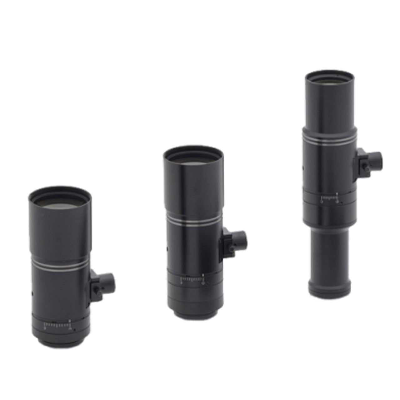
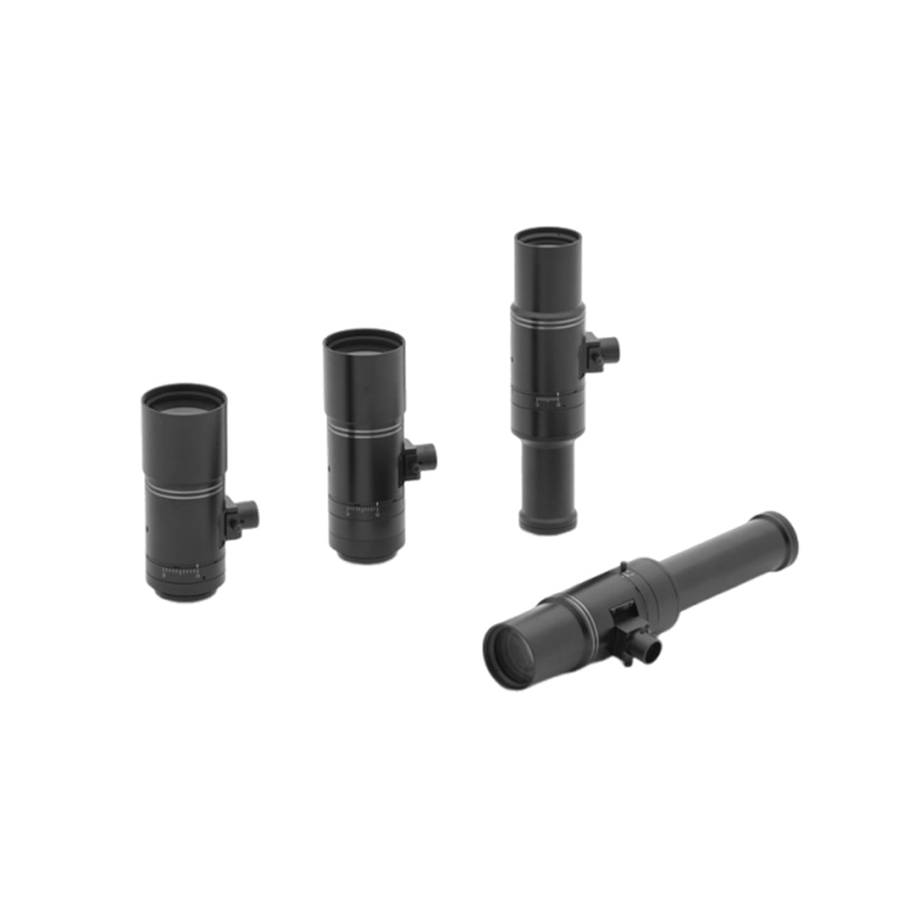
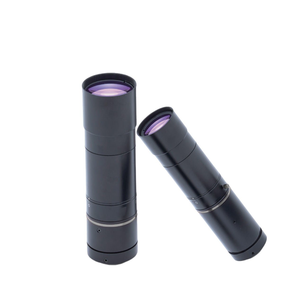
A: The TLVS-H1.1 is a Visible–SWIR telecentric lens series designed for semiconductor inspection, IC imaging, silicon transmission analysis, and multi-spectral machine vision applications.
Q2: What is focus shift correction in this lens?
A: Focus shift correction allows the lens to maintain consistent focus across 400–1200nm wavelengths, eliminating the need to refocus when switching between visible and SWIR imaging.
Q3: Can this lens capture internal structures through silicon?
A: Yes. At around 1100nm transmission wavelength, the lens can image internal IC circuits and structures through silicon wafers.
Q4: What magnification options are available?
A: The series supports 0.7X, 1.0X, 2.0X, and 4.0X magnifications, suitable for different inspection and measurement requirements.
Q5: What is the advantage of a telecentric design?
A: Telecentric optics ensure low distortion, stable magnification, and high measurement accuracy, which is essential for precision inspection.
Q6: Does the lens support both coaxial and non-coaxial setups?
A: Yes, the TLVS-H1.1 series is available in coaxial and non-coaxial versions, depending on the application environment.
Q7: What industries commonly use this lens?
A: It is widely used in semiconductor manufacturing, IC inspection, electronics production, precision metrology, and advanced machine vision systems.
Q8: What is the wavelength range of this lens?
A: The lens operates across a wide 400–1200nm spectral range, covering both visible and SWIR imaging.


Estimated Delivery Time

Ship To Detecting...
Delivery: -
説明
製品説明
精密イメージング向け、焦点シフト補正付き可視光~SWIRテレセントリックレンズ
TLVS-H1.1シリーズは、400nmから1200nmまでの広い波長範囲でのイメージングを要求する高度なマシンビジョンアプリケーション向けに設計された、高性能な可視光~SWIRテレセントリックレンズです。独自の焦点シフト補正技術により、可視光から短波長赤外線(SWIR)まで一貫した画像焦点を確保し、マルチスペクトル検査時の再焦点合わせの必要性を排除します。
このシリーズは、高い安定性で可視光画像と透過SWIR画像の両方をキャプチャ可能であり、標準的な可視光イメージングでは見えない内部構造や欠陥の検出を可能にします。特に、シリコンウェハ検査や約1100nmの透過波長でのIC内部回路イメージングに効果的です。
0.7X、1.0X、2.0X、4.0Xの倍率で利用可能なTLVS-H1.1シリーズは、同軸型と非同軸型の両方の構成に対応しており、異なる産業用検査システムへの柔軟な統合を提供します。
主な特徴
✔ 可視光~SWIR広帯域イメージング(400–1200nm)
可視光からSWIRスペクトルまでシームレスなイメージングをサポートします。
✔ 焦点シフト補正技術
調整なしで複数の波長にわたってシャープな焦点を維持します。
✔ テレセントリック光学設計
歪みのないイメージングと高い測定精度を確保します。
✔ マルチ倍率オプション(0.7X–4.0X)
さまざまなマシンビジョンアプリケーションに対応する柔軟な構成です。
✔ ICシリコン透過イメージング(約1100nm)
シリコンウェハを介した内部回路の検査を可能にします。
✔ 同軸型 / 非同軸型をご用意
反射型および透過型検査システムに適しています。
推奨アプリケーション
- 半導体ウェハ検査
- IC内部回路イメージング
- シリコン透過検査
- 電子機器製造
- スペクトル横断的な欠陥検出
- 精密計測
- 高度なマシンビジョンシステム
- マルチスペクトル産業用イメージング
仕様
400-1200nm VIS-SWIR Cマウント テレセントリックレンズ
| モデル | 倍率 | 作業距離 | 像円 | 同軸型 |
|---|---|---|---|---|
| TLVS-0.7XD-H1.1 | 0.7X | 110 mm | Φ20.5 mm | はい |
| TLVS-0.7X-H1.1 | 0.7X | 110 mm | Φ20.5 mm | いいえ |
| TLVS-1.0XD-H1.1 | 1.0X | 110 mm | Φ24 mm | はい |
| TLVS-1.0X-H1.1 | 1.0X | 110 mm | Φ24 mm | いいえ |
| TLVS-2.0XD-H1.1 | 2.0X | 110 mm | Φ24 mm | はい |
| TLVS-2.0X-H1.1 | 2.0X | 110 mm | Φ24 mm | いいえ |
| TLVS-4.0XD-H1.1 | 4.0X | 110 mm | Φ20.5 mm | はい |
| TLVS-4.0X-H1.1 | 4.0X | 110 mm | Φ20.5 mm | いいえ |
SWIRレンズダウンロード

発送予定
Payment & Security
お支払い情報は安全に処理されます。 クレジットカードの詳細を保存したり、クレジットカード情報にアクセスすることはありません