
1. What is the iBt-UV9KT used for?
The iBt-UV9KT is designed for silicon wafer inspection, semiconductor surface inspection, wafer defect detection, and high-speed automated imaging.
2. Why use UV imaging for silicon wafer inspection?
UV imaging can provide additional material and surface information that may not be easily captured with visible-light imaging, making it useful for specialized wafer inspection applications.
3. What is the resolution of the iBt-UV9KT?
The camera provides 9072 × 256 resolution with 5 μm pixels, supporting detailed line scan imaging for silicon wafer inspection.
4. How does 256-TDI improve wafer inspection?
The 256-TDI structure accumulates optical signals across multiple stages during scanning, increasing effective sensitivity and helping capture subtle features during high-speed wafer inspection.
5. Is the iBt-UV9KT suitable for automated wafer inspection systems?
Yes. Its high line rate, 9K resolution, CXP12 interface, and TDI architecture make it suitable for integration into automated semiconductor and wafer inspection equipment.
6. What optical configuration can be used with the iBt-UV9KT?
The camera uses an M72 lens mount and can be integrated with suitable UV optics selected according to the wafer size, field of view, working distance, and inspection requirements.



Estimated Delivery Time

Ship To Detecting...
Delivery: -
Description
Product Description
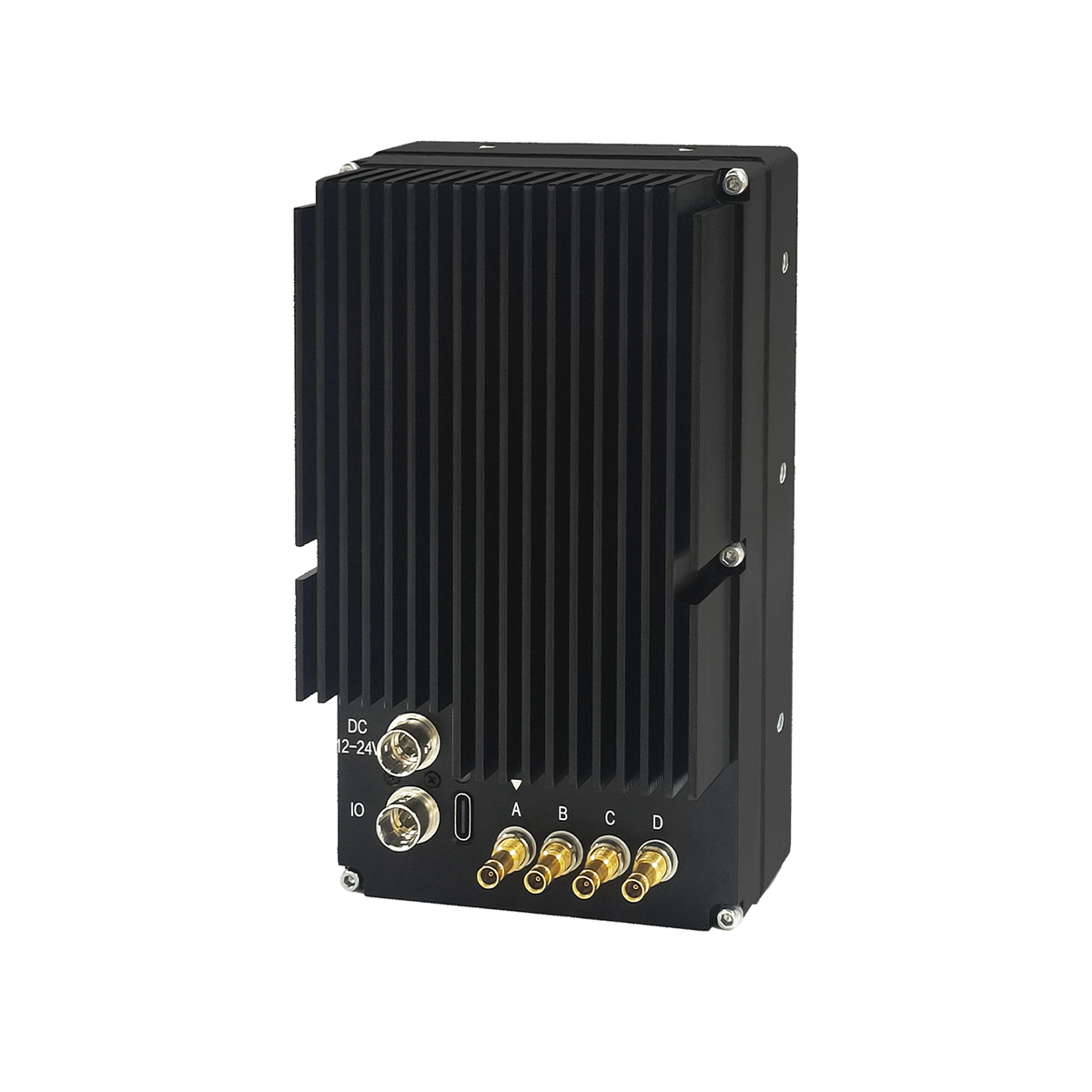
The iBt-UV9KT is a high-resolution 9K UV TDI line scan camera designed for silicon wafer inspection and semiconductor imaging. With 9072 × 256 resolution, 256-TDI, 5 μm pixels, and a 529.4 kHz line rate, it provides high-sensitivity UV imaging for demanding wafer inspection systems.
Its 256-TDI architecture enhances signal accumulation for detecting fine surface features and weak UV signals. Combined with a CXP12 interface and M72 lens mount, the camera supports high-speed data transmission and flexible optical integration for automated silicon wafer and semiconductor inspection.
Key Features
✔ 9K UV Resolution: 9072 × 256 for detailed wafer imaging
✔ 256-TDI: Enhanced sensitivity for fine wafer inspection
✔ 529.4 kHz Line Rate: High-speed line scan acquisition
✔ 5 μm Pixels: High spatial resolution for surface inspection
✔ CXP12 Interface: High-bandwidth industrial imaging
Typical Applications
- Silicon Wafer Inspection
- Semiconductor Inspection
- Wafer Surface Inspection
- Wafer Defect Detection
- Micro-Defect Inspection
- Semiconductor Manufacturing
- UV-Based Material Inspection
- Automated Wafer Inspection
Specifications
| Model | iBt-UV9KT |
| Resolution | 9072 × 256 |
| TDI | 256-TDI |
| Line Rate | 529.4 kHz |
| Pixel Size | 5 μm |
| Interface | CXP12 |
| Lens Mount | M72 |
| Camera Type | UV TDI Line Scan |

Estimate shipping
Payment & Security
Your payment information is processed securely. We do not store credit card details nor have access to your credit card information.