
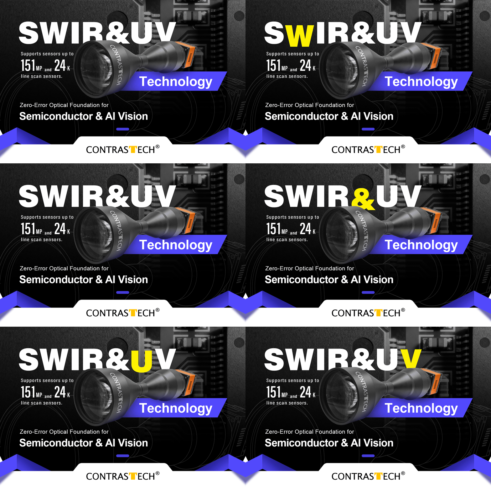
เมื่อข้อผิดพลาดไม่ใช่ทางเลือก
เลนส์เทเลเซ็นทริกเป็นรากฐานทางแสงเบื้องหลังการตรวจสอบเซมิคอนดักเตอร์สมัยใหม่ การวัดความแม่นยำ และระบบวิทัศน์ AI
ในสภาพแวดล้อมการผลิตขั้นสูง ความแม่นยำของภาพกำหนดความน่าเชื่อถือของผลการตรวจสอบ หากระบบแสงทำให้เกิดความผิดเพี้ยน การเปลี่ยนแปลงของกำลังขยาย หรือสิ่งรบกวนจากการสะท้อน แอลกอริทึมขั้นสูงที่สุดก็ไม่สามารถชดเชยข้อผิดพลาดที่ต้นทางได้
นี่คือจุดที่ เลนส์เทเลเซ็นทริก กลายเป็นสิ่งสำคัญ
ระบบแสงเทเลเซ็นทริกขจัดข้อผิดพลาดเชิงทัศนียภาพ เสถียรภาพกำลังขยาย และให้ภาพที่ปราศจากความผิดเพี้ยน—ซึ่งให้รากฐานทางภาพที่เชื่อถือได้สำหรับ การตรวจสอบ การวัดความแม่นยำ และข้อมูลฝึกสอน AI.
ทำไมเลนส์ อุตสาหกรรมทั่วไป จึงกำลังกลายเป็นคอขวด

การตรวจสอบเซมิคอนดักเตอร์
ความเบี่ยงเบนทางเรขาคณิตระดับไมครอนอาจนำไปสู่การจำแนกข้อบกพร่องที่ไม่ถูกต้อง แม้ ความผิดเพี้ยนทางแสงเพียงเล็กน้อยสามารถเพิ่มอัตราการตัดสินข้อบกพร่องผิดพลาดได้อย่างมีนัยสำคัญ.
การวัดความแม่นยำ
เมื่อตำแหน่งของวัตถุเคลื่อนที่เล็กน้อย เลนส์ทั่วไปจะก่อให้เกิดการเปลี่ยนแปลงเชิงทัศนียภาพ ทำให้ ผลการวัดมีความผันผวน.
การตรวจสอบพื้นผิวสะท้อนแสง
วัสดุที่มีลักษณะเหมือนกระจกมักทำให้เกิด จุดสว่างที่สว่างจ้าเกินไป, สร้างจุดบอดในการตรวจสอบคุณภาพ
การฝึกสอนวิทัศน์ AI
หากข้อมูลฝึกสอนมาจากภาพที่ผิดเพี้ยน ตัวโมเดล AI เองก็จะถูกกระทบ.
เลนส์เทเลเซ็นทริกคืออะไร และทำไมจึงสำคัญ
เลนส์เทเลเซ็นทริกถูกออกแบบให้รังสีหลักเดินทาง ขนานกับแกนแสง. โครงสร้างทางแสงนี้ขจัดความผิดเพี้ยนเชิงทัศนียภาพและรักษาความคงที่ของกำลังขยายทั่วทั้งสนามภาพ
สิ่งนี้ทำให้สามารถ:
- ข้อผิดพลาดเชิงทัศนียภาพเป็นศูนย์
- กำลังขยายคงที่
- ความผิดเพี้ยนต่ำมาก
- การวัดที่ซ้ำได้สูง
เลนส์เทเลเซ็นทริกถูกใช้อย่างแพร่หลายใน:
- การตรวจสอบเวเฟอร์เซมิคอนดักเตอร์
- การตรวจสอบแผง PCB และ LCD
- ระบบวัดความแม่นยำ
- แพลตฟอร์มฝึกสอนวิทัศน์ AI
- การตรวจสอบแบตเตอรี่ลิเธียม
- การคัดแยกวัสดุขั้นสูง
ทำไมต้องเลือกเลนส์เทเลเซ็นทริกจาก Contrastech
การออกแบบทางแสงที่มีความผิดเพี้ยนต่ำมาก
ระดับความผิดเพี้ยนต่ำถึง ≤0.01%, ตอบสนองความต้องการการตรวจสอบระดับเซมิคอนดักเตอร์
รองรับเซ็นเซอร์ความละเอียดสูงมาก
- เข้ากันได้กับ เซ็นเซอร์แบบพื้นที่สูงสุด 151MP
- รองรับ กล้องสแกนแบบเส้น 24K
สนามภาพขนาดใหญ่พิเศษ
สนามภาพสูงสุดถึง 390 mm, เหมาะสำหรับการตรวจสอบ PCB ขนาดใหญ่ การตรวจสอบ LCD และการวิเคราะห์วัสดุพื้นที่ขนาดใหญ่
ความเข้ากันได้ของเซ็นเซอร์ที่หลากหลาย
รองรับขนาดเซ็นเซอร์ตั้งแต่ 1/2.5", 1", 2/3", APS-C ถึงฟูลเฟรม โดยมีวงกลมภาพสูงสุดถึง 88 mm.
ช่วงกำลังขยายที่กว้าง
ตัวเลือกกำลังขยายตั้งแต่ 0.024X – 8X, รองรับทั้งการตรวจสอบแบบมาโครและการวัดระดับไมครอน
ทางออกด้านสเปกตรัมขั้นสูง
เทเลเซ็นทริก UV
- การตรวจสอบเซมิคอนดักเตอร์
- การตรวจจับรอยร้าวขนาดเล็ก
- การวัดความแม่นยำ
เทเลเซ็นทริก SWIR
- การตรวจสอบการทะลุผ่านวัสดุ
- การวิเคราะห์เวเฟอร์ซิลิคอน
- การตรวจสอบการห่อหุ้มอิเล็กทรอนิกส์
ไบ-เทเลเซ็นทริก
- การวัดขนาดระดับซับพิกเซล
- ระบบวัดความแม่นยำ
- วิทัศน์เครื่องจักรที่เสถียรสูง
คำติชมจากอุตสาหกรรม
วิธีเลือกเลนส์เทเลเซ็นทริกให้เหมาะสม
- ขนาดเซ็นเซอร์
- ความแม่นยำในการวัดที่ต้องการ
- สนามภาพ
- ข้อกำหนดด้านสเปกตรัม (UV / Visible / SWIR)
- จำเป็นต้องใช้ระบบแสงไบ-เทเลเซ็นทริกหรือไม่
หากไม่มีการจับคู่ที่เหมาะสม แม้แต่ระบบวิทัศน์ระดับสูงก็อาจไม่สามารถบรรลุประสิทธิภาพที่คาดหวังได้

ค้นหาโซลูชันเทเลเซ็นทริกที่เหมาะสม
Contrastech สามารถช่วยออกแบบโซลูชันทางแสงเทเลเซ็นทริกที่เหมาะสมที่สุดสำหรับการตรวจสอบเซมิคอนดักเตอร์ ระบบวิทัศน์ AI และการวัดความแม่นยำ
ติดต่อเราสำหรับแอปพลิเคชันของคุณ